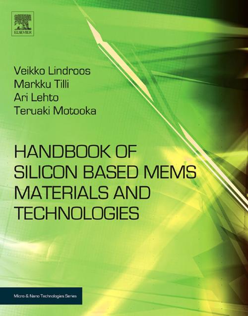
Handbook of Silicon Based MEMS Materials and Technologies
Nonfiction, Science & Nature, Technology, Electronics, Microelectronics, Material Science| Author: | ISBN: | 9780815519881 | |
| Publisher: | Elsevier Science | Publication: | December 8, 2009 |
| Imprint: | William Andrew | Language: | English |
| Author: | |
| ISBN: | 9780815519881 |
| Publisher: | Elsevier Science |
| Publication: | December 8, 2009 |
| Imprint: | William Andrew |
| Language: | English |
A comprehensive guide to MEMS materials, technologies and manufacturing, examining the state of the art with a particular emphasis on current and future applications.
Key topics covered include:
- Silicon as MEMS material
- Material properties and measurement techniques
- Analytical methods used in materials characterization
- Modeling in MEMS
- Measuring MEMS
- Micromachining technologies in MEMS
- Encapsulation of MEMS components
- Emerging process technologies, including ALD and porous silicon
Written by 73 world class MEMS contributors from around the globe, this volume covers materials selection as well as the most important process steps in bulk micromachining, fulfilling the needs of device design engineers and process or development engineers working in manufacturing processes. It also provides a comprehensive reference for the industrial R&D and academic communities.
- Veikko Lindroos is Professor of Physical Metallurgy and Materials Science at Helsinki University of Technology, Finland.
- Markku Tilli is Senior Vice President of Research at Okmetic, Vantaa, Finland.
- Ari Lehto is Professor of Silicon Technology at Helsinki University of Technology, Finland.
- Teruaki Motooka is Professor at the Department of Materials Science and Engineering, Kyushu University, Japan.
• Provides vital packaging technologies and process knowledge for silicon direct bonding, anodic bonding, glass frit bonding, and related techniques
• Shows how to protect devices from the environment and decrease package size for dramatic reduction of packaging costs
• Discusses properties, preparation, and growth of silicon crystals and wafers
• Explains the many properties (mechanical, electrostatic, optical, etc), manufacturing, processing, measuring (incl. focused beam techniques), and multiscale modeling methods of MEMS structures
